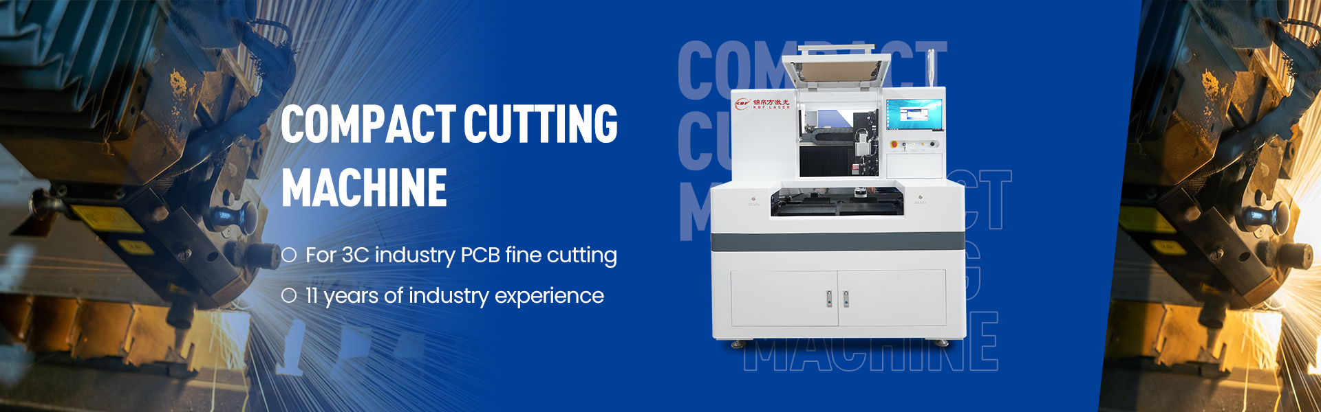


Description
Specification
Video
Application
Description
Let’s have a short appear at the fundamental advantages of the use of a PCB laser marking computing device over different current strategies of labeling.
- Cost-Effective: Laser marking of PCBs prices extensively decrease than the equal quantity of labeling executed by means of ink/chemicals.
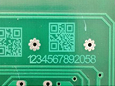
- Clarity of Label: The ultimate effects of PCB marking are significantly one-of-a-kind for Ink/Stickers and Laser markings. The ink/sticker marks are now not very clear and can create trouble through guide or scanner reading. On the other hand, the laser markings on PCBs create crystal clear markings that are handy to study by using the bare eye and digital scanners.
- Time-Saving: The laser marking of PCBs is a wholly computerized system that saves time and labor and produces enormously environment friendly results.
- Easy to Use: The utterly computerized system helps you deal with the marking method like any different conveyor processing system. The totally computerized conveyor machine makes it viable for you bulk-print your PCBs simply through the click on of a single button.
- The durability of the Marking: Ink markings and stickers have a tendency to lose their illegibility over time. Whereas, the laser marking is everlasting and is nevertheless very clear after ten to fifteen years of use.
- Environment-Friendly Marking Scheme: Most of the marking inks that are normally used for PCB markings are now not environment-friendly. Whereas, when you use the laser marking methodology for PCBs, there is no waste.
Specification
| Product model | KBF-UV300-PA | KBF-UV450-PA | KBF-UV450G-PA | KBF-UV600-PA | ||||
| Laser type | CO2/UV | CO2/UV | CO2/UV | CO2/UV | ||||
| How it works | The laser is fixed | The laser moves | The laser moves | The laser moves | ||||
| Output wavelength | 10.6um | 355nm | 10.6um | 355nm | 10.6um | 355nm | 10.6um | 355nm |
| Laser power | 5w/10w/30w | 3w | 5w/10w/30w | 3w | 5w/10w/30w | 3w | 5w/10w/30w | 3w |
| Minimum line width | 0.1mm | 0.01mm | 0.1mm | 0.01mm | 0.1mm | 0.01mm | 0.1mm | 0.01mm |
| Beam quality M ² | ≤1.8 | ≤1.2 | ≤1.8 | ≤1.2 | ≤1.8 | ≤1.2 | ≤1.8 | ≤1.2 |
| Laser spot | 0.17mm/0.11 | ≤0.8 | 0.17mm/0.11 | ≤0.8 | 0.17mm/0.11 | ≤0.8 | 0.17mm/0.11 | ≤0.8 |
| Cooling method | Air Cooling | Water/Air Cooling | Air Cooling | Water/Air Cooling | Air Cooling | Water/Air Cooling | Air Cooling | Water/Air Cooling |
| Maximum PCB dimension | 300mmX300mm | 450mmX450mm | 450mmX450mm | 600mmX600mm | ||||
| PCB marking range | 300mmX300mm | 450mmX450mm | 450mmX450mm | 600mmX600mm | ||||
| Marking range | 50mmX50mm | |||||||
| 180mmX180mm | ||||||||
| 300mmX300mm | ||||||||
| 450mmX450mm | ||||||||
| Repeated positioning accuracy | ±25μm | |||||||
| Transmission height | 920± 20mm | |||||||
| Minimum Engraving Size | 2.5X2.5mm | |||||||
| Positioning system | CCD + MARK coordinate positioning and correction | |||||||
| Code reading system | CCD | |||||||
| Drive mode | AC servo motor system | |||||||
| Track width adjustment | Automatic width adjustment system | |||||||
| Conveying speed | Adjustable speed, 500 mm/Smax | |||||||
| Transmission direction | Left to right or right to left, optional | |||||||
| The PCB is allowed to deform | ±1mm | |||||||
| PCB thickness | 0.5-5mm | |||||||
| PCB passing height | UP:20mm DOWN:20mm | |||||||
| Smoke treatment method | Smoke purification system | |||||||
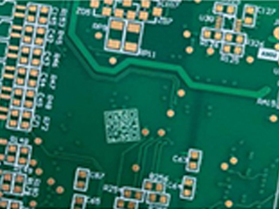
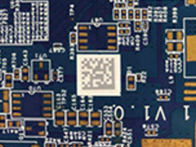
| Engraving content | Text, QR code and graphics | |||||||
| Operating System | WIN10 + KBF software | |||||||
| Foolproof system | PCB reverse/back side automatic identification | |||||||
| System docking | Can be connected to MES/IMS/PMS and other systems | |||||||
| Operating voltage | 220v±10% 50/60HZ | |||||||
| Air pressure source | 0.4~0.6MPA | |||||||
| Environmental requirements | Temperature 10~30℃ | |||||||
| Humidity 30~80%RH | ||||||||
| Equipment power | 2.5 KVA | |||||||
| Communication interface | SMEMA | |||||||
| Size of equipment | L1658XW1650XH1700mm | L980XW1660XH1550mm | L980XW1660XH1550mm | L1150XW1540XH1500mm | ||||
| Equipment weight | 750KG | 850KG | 900KG | 950KG | ||||
Video
Application
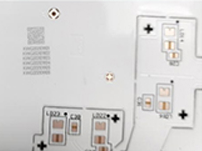
PCB laser marking system working process:


- Preparation: Before starting the marking process, the PCB must be cleaned and positioned correctly in the laser marking machine. The laser marking software is then used to create a QR code image that will be marked on the PCB.
- Marking: The laser beam is focused on the area of the PCB where the QR code is to be marked. The laser then generates pulses of energy, which ablate the PCB material, leaving a permanent mark. The laser parameters are set to ensure a high-quality mark that is clear, precise, and readable by scanning devices.
- Verification: After the marking is complete, the QR code is scanned to verify that it is accurate and readable. This ensures that the PCB is correctly identified and tracked throughout the manufacturing process.